
Earlier this year, AMD made it very clear that they wanted to challenge Intel in several market segments. The first fight was over low power, light weight laptops with the launch of the AMD E-350 which took on the Intel Atom. It was a grueling match that ended in a split decision for AMD. Now it is time for the mainstream desktop championship to be put on the line against AMD’s new A8-3850/A6-3650 APUs and their new corner man, the Hudson FCH. Does AMDs new contender have what it takes to take the title belt?
The Llano APU Architecture
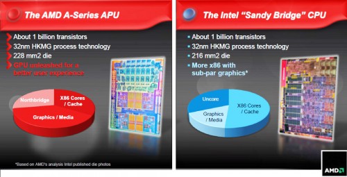
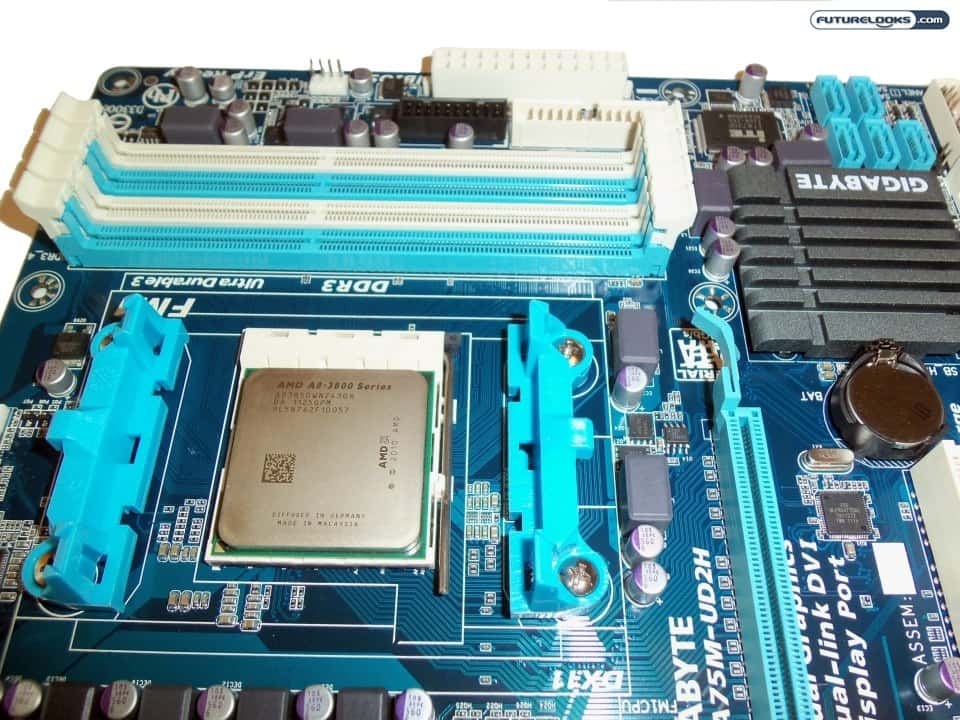
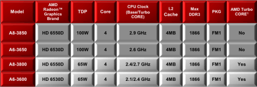
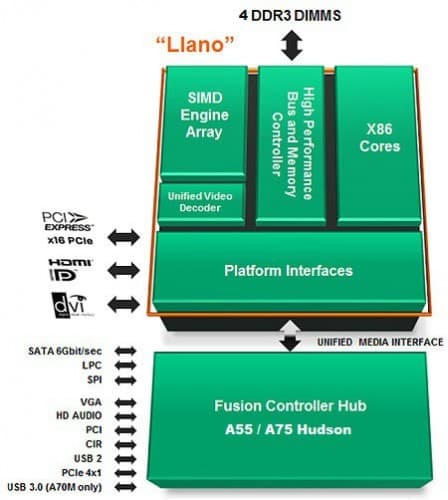
Code named Llano, you can easily see why AMD calls this chip design an APU (Accelerated Processing Unit). It combines a 32nm K10 “Stars” based CPU, up to 400 Radeon 6000 series SIMDs, and now the entire northbridge. While similar in design to the Intel Sandy Bridge, AMD is more balanced in their approach. The APU lineup is below and I will be testing both the A8-3850 and A6-3650 in this review.
On-Die Graphics
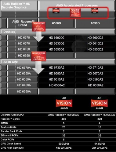
The GPU portion of AMD Llano is nearly half of the chip and promises entry level discrete card performance. This is a very smart move on AMDs part as weak graphics are one of the first things you notice about entry level PCs. This is also the one area AMD has a huge advantage over Intel. In this review, we will test two variations of the “Sumo” Radeon chip in the 6550D and 6530D.
When you compare the “Sumo” GPUs to other offerings from AMD, their name and specs put them between the AMD 6450 and AMD 6570 dedicated cards. The “D” stands for desktop, but is mainly just to distinguish these as not being a dedicated card. Also in the chart you will notice the “Sumo” GPUs can be linked via CrossFireX to dedicated cards in the same performance range. This is a great feature, as those who buy an entry level dedicated card will get more than what they pay for paired up with an A75 board and APU.
On-Die CPU and Northbridge
There is nothing really new to the CPU side of the A8-3850 and A6-3650. It is a “Stars” core design from the AMD K10 block of CPUs. It has been shrunk down to 32nm and uses HKMG (High-K Metal Gates). These cores come with 1 MB of L2 cache instead of the 512 KB you find on other K10 chips like the Athlon II. These seemingly minor updates should push the APU performance north of similar quad-core K10 “Propus” CPUs.
The final piece of the APU architecture is how it communicates with the world. AMD has used an on-die memory controller for almost a decade, but this is of a different breed. The A8-3850 and A6-3650 both support up to 4 DDR3 DIMMs up to 1866 MHz, though AMD has cautioned that official support is only for two DIMMs at this clock speed. The APU shares resources with the on-die GPU with the most noticeable being the memory controller.
New to AMD is the on-die northbridge which is responsible for video output, PCIe graphics, and southbridge communication. The APUs can handle one each of a DisplayPort 1.1a, 1.4a HDMI port, DVI-D, and legacy VGA via a 4x PCIe lane. It can handle up to 3 displays in Eyefinity at 1080p or a single display up to 2560 x 1600. The APUs also have one 16x PCIe and up to four 1x PCIe lanes (which can be combined into a single 4x PCIe lane). Including the four PCIe lanes used for the display output, this makes up all of the APUs 24 PCIe lanes.
The final task of the on-die northbridge is communication with the southbridge. This comes in the form of a single link from the APU to the Hudson FCH (Fusion Controller Hub). The UMI 2.0 or Unified Media Interface 2.0 is clocked normally at 2.0 GHz and transmits 2 GB/s of data. This is the same bandwidth as a PCIe 2.0 4x link. Now lets take a look at the Hudson FCH which takes the place of a southbridge.