Earlier this year, AMD made it very clear that they wanted to challenge Intel in several market segments. The first fight was over low power, light weight laptops with the launch of the AMD E-350 which took on the Intel Atom. It was a grueling match that ended in a split decision for AMD. Now it is time for the mainstream desktop championship to be put on the line against AMD’s new A8-3850/A6-3650 APUs and their new corner man, the Hudson FCH. Does AMDs new contender have what it takes to take the title belt?
The Llano APU Architecture
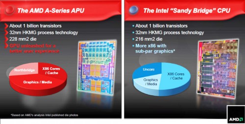

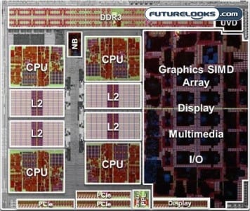
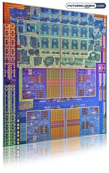
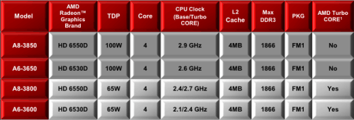
Code named Llano, you can easily see why AMD calls this chip design an APU (Accelerated Processing Unit). It combines a 32nm K10 “Stars” based CPU, up to 400 Radeon 6000 series SIMDs, and now the entire northbridge. While similar in design to the Intel Sandy Bridge, AMD is more balanced in their approach. The APU lineup is below and I will be testing both the A8-3850 and A6-3650 in this review.

On-Die Graphics
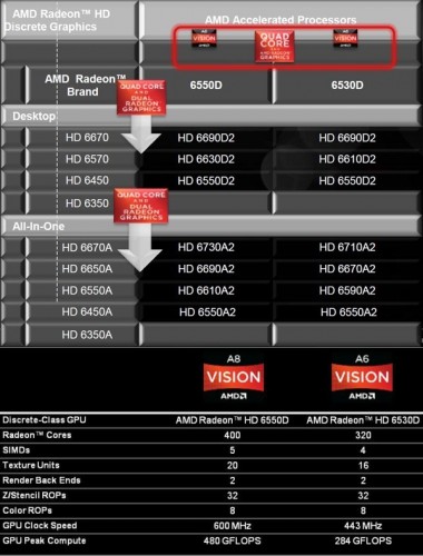

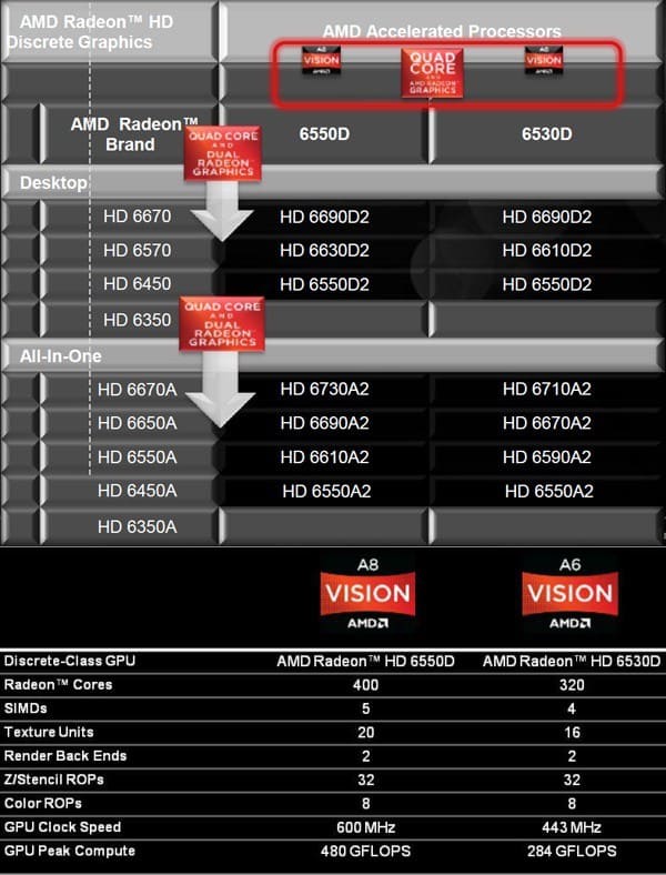
The GPU portion of AMD Llano is nearly half of the chip and promises entry level discrete card performance. This is a very smart move on AMDs part as weak graphics are one of the first things you notice about entry level PCs. This is also the one area AMD has a huge advantage over Intel. In this review, we will test two variations of the “Sumo” Radeon chip in the 6550D and 6530D.
When you compare the “Sumo” GPUs to other offerings from AMD, their name and specs put them between the AMD 6450 and AMD 6570 dedicated cards. The “D” stands for desktop, but is mainly just to distinguish these as not being a dedicated card. Also in the chart you will notice the “Sumo” GPUs can be linked via CrossFireX to dedicated cards in the same performance range. This is a great feature, as those who buy an entry level dedicated card will get more than what they pay for paired up with an A75 board and APU.
On-Die CPU and Northbridge

There is nothing really new to the CPU side of the A8-3850 and A6-3650. It is a “Stars” core design from the AMD K10 block of CPUs. It has been shrunk down to 32nm and uses HKMG (High-K Metal Gates). These cores come with 1 MB of L2 cache instead of the 512 KB you find on other K10 chips like the Athlon II. These seemingly minor updates should push the APU performance north of similar quad-core K10 “Propus” CPUs.
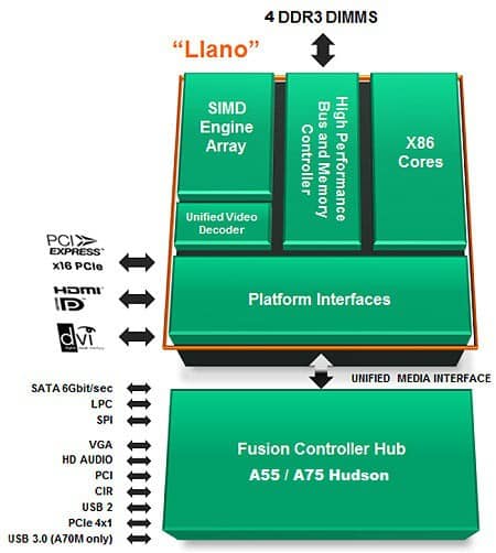
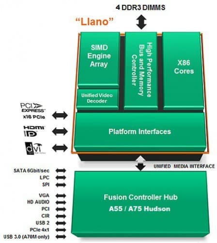
The final piece of the APU architecture is how it communicates with the world. AMD has used an on-die memory controller for almost a decade, but this is of a different breed. The A8-3850 and A6-3650 both support up to 4 DDR3 DIMMs up to 1866 MHz, though AMD has cautioned that official support is only for two DIMMs at this clock speed. The APU shares resources with the on-die GPU with the most noticeable being the memory controller.
New to AMD is the on-die northbridge which is responsible for video output, PCIe graphics, and southbridge communication. The APUs can handle one each of a DisplayPort 1.1a, 1.4a HDMI port, DVI-D, and legacy VGA via a 4x PCIe lane. It can handle up to 3 displays in Eyefinity at 1080p or a single display up to 2560 x 1600. The APUs also have one 16x PCIe and up to four 1x PCIe lanes (which can be combined into a single 4x PCIe lane). Including the four PCIe lanes used for the display output, this makes up all of the APUs 24 PCIe lanes.
The final task of the on-die northbridge is communication with the southbridge. This comes in the form of a single link from the APU to the Hudson FCH (Fusion Controller Hub). The UMI 2.0 or Unified Media Interface 2.0 is clocked normally at 2.0 GHz and transmits 2 GB/s of data. This is the same bandwidth as a PCIe 2.0 4x link. Now lets take a look at the Hudson FCH which takes the place of a southbridge.
Hudson FCH A55/A75
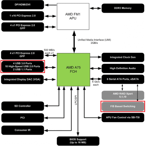

The Fusion Controller Hub provides the APU design platform all of the bullet point features. The A75 has support for up to six 6Gb/s SATA (with FIS-based switching), 4 USB 3.0, up to 10 USB 2.0, up to 2 USB 1.1a, four 1x PCIe lanes and up to 3 legacy PCI ports. The FCH handles other functions such as clock generation, APU fan controls, and VGA DAC. Bonus features are included as well such as a consumer IR and SD controller. All of this is on top of the standard features of BIOS access, Ethernet ports, and an HD audio controller.
The only difference in the A55 is the lack of USB 3.0 support (up to 14 USB 2.0 ports instead) and no FIS-based switching. The combination of the Hudson FCH and the AMD APU for desktops is called the “Lynx” platform. For now, we will look at the Llano APUs. We have the A8-3850 with an MSRP of $139.99 and the A6-3650 with an MSRP of $119.99.
Test Setup and Installation Notes
APU Test System
- CPU: AMD A8-3850 & A6-3650
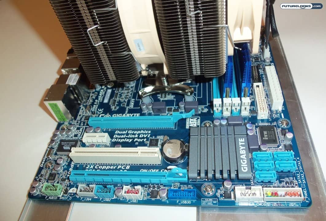
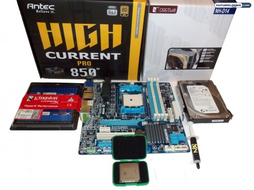
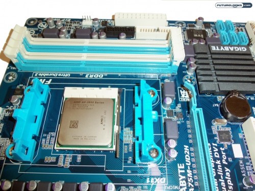
- Motherboard: GIGABYTE A75M-UD2H
- Memory: Kingston HyperX 1600 MHz 9-9-9-24 T1 DDR3 (2x2GB)
- HDD: Seagate Barracuda XT 2TB 7200 RPM
- GPU: On-die 6550D, On-die 6530D, and dedicated GIGABYTE HD 6670 1 GB
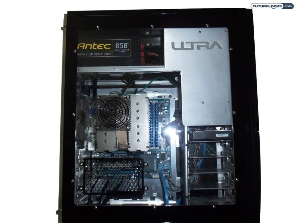
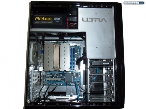
- PSU: Antec HCP 850 Watt 80+ Gold
- Cooler: Noctua NH-D14 (with 1 x 140 mm fan)
APU Test System Overclocked
- A8-3850 @ 3.57 GHz with 6550D @ Stock
- A6-3650 @ 3.43 GHz with 6530D @ 600 MHz (Stock of 444 MHz)
- Memory @ 1760 MHz 9-9-9-24 T1
Phenom II System
- CPU: AMD Phenom II 955 @ 3.2 GHz
- Motherboard: MSI 790GX-G65
- Memory: Kingston HyperX 1333 MHz 7-7-7-21 T1 DDR3 (2x2GB)
- HDD: Samsung SpinPoint F3 1 TB
- GPU: GIGABYTE HD 6670 1 GB
- PSU: Antec HCP 850 Watt 80+ Gold
- Cooler: Scythe Mugen II Rev. B
Software Used
AIDA64, AMD Resource Monitor, OCCT, FurMark Burn Test, Sandra Lite 2011 SP4a, 3DMark11, Alien vs. Predator DX11 benchmark, Resident Evil 5 Benchmark, Portal 2, Fraps 3.4.6, Handbrake 0.9.4, Media Espresso 6.5, and CINEBENCH 11.5
First, the Phenom II rig is my personal computer with the exception of the RAM, GPU, and PSU. While not as controlled as I would like, I think it provides a better picture of of how AMD is moving forward with their platforms and chip designs. The difference in memory speed and timing is due to the Phenom II 955 losing performance at 1600 MHz with CAS 9. At 1333 MHz CAS 7, I gain a full 1.1 GB/s memory bandwidth for the Phenom II system.
The only issue you may encounter with a build using an APU and FM1 socket board is if you add a dedicated GPU later. Windows will at first not recognize the new GPU as being an AMD card. This is easily fixed with a restart after the first boot. This same issue comes up with swapping the APUs as well, but the CPU portion of the chips is recognized immediately.
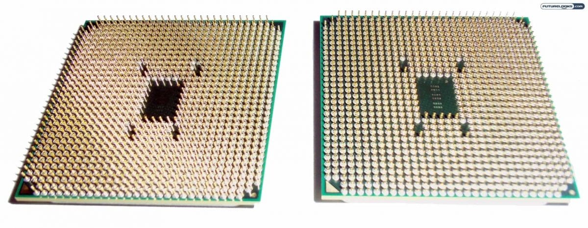
One other thing that some folks are wondering is whether or not they’ll be throwing away their AM3 or AM2+ CPU coolers. The answer is anything that fit AM2+ or AM3 will fit on the FM1 socket. So if you have a great silent cooler, it’ll be right at home on the A75 and A55 platforms on top of the new APUs.
APU Special Testing
Since the APUs are both a CPU and GPU, I decided to start testing with a few special test to minimize variables. I tested the UMA buffer (memory dedicated to the on-die GPU), on-die GPU clock speed, memory speed, and memory timing to see which could drastically affect scores.
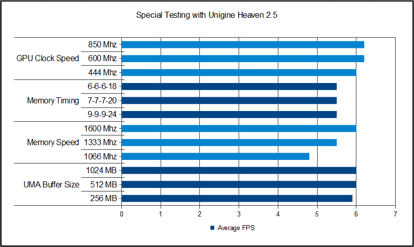
The UMA buffer size of 256 MB does choke the GPU a little with a 3.3% lose in performance. The same can be said for the on-die GPU clock rate below 600 MHz. Neither of these are the limiting factor in performance which is why AMD set the clock of the 6550D to 600 MHz. Memory timing affects nothing at all. Even when tested with AIDA64 it only provides below 50 MB/s improvements.
The major factor in performance comes from memory speed. You gain 12.73% performance going from 1066 MHz to 1333 MHz, and another 8.33% from 1333 MHz to 1600 MHz. It is good to see the APUs benefit much more from memory speed and timing. Something that was not a factor with the Phenom II platform.
Although I could not test 1866 MHz speed at this time, consider 1600 MHz RAM is currently far more common and extremely cheap. As of writing this review, there are only 22 DDR3 1866 MHz memory kits and over 200 DDR3 1600 MHz kits available for purchase at a single major PC parts retailer. This means most people who buy an AMD A8-3850 or A6-3650 will likely be using 1600 MHz RAM.
CINEBENCH 11.5 CPU Benchmark
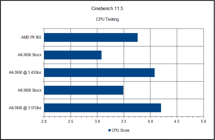
CINEBENCH 11.5 CPU test is about performance plain and simple. The A8-3850 and A6-3650 are based on the same K10 Architecture as the Phenom II 955. This results in the higher the clock speed, the better the score in this test.
Sandra Lite 2011 SP4a
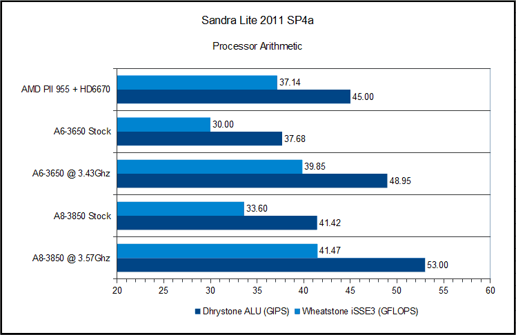
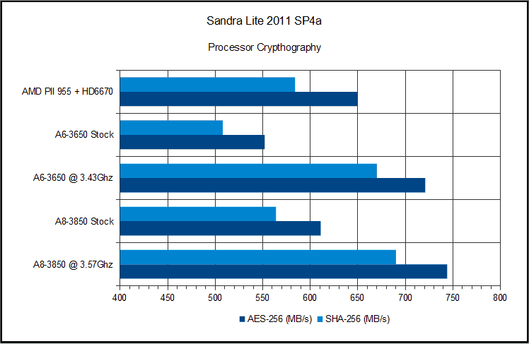
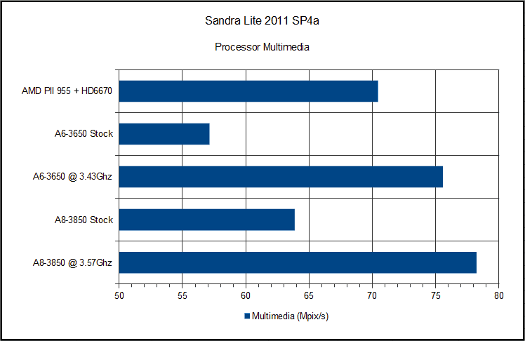
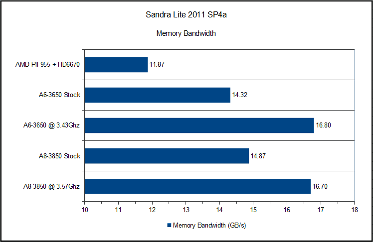
In every performance test, there are no surprises. The A8-3850 and A6-3650 fall right in line. The faster the clock rate, the more performance you will get. The one exception being Memory bandwidth in which even the slower A6-3650 has a 2.45 GB/s advantage over the Phenom II 955. This is a minimum of 20.64% bandwidth improvement from the new memory controller.
Handbrake 0.9.4 CPU Conversion
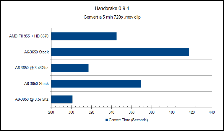
In the Handbrake test I converted a 5 minute 720p .mov H.264 clip using the iPhone4 preset. As with the synthetic tests, real world performance is the same story. The high the clock rate, the faster the encoding is done. It is very clear the CPU side of these APUs are based on the same “Stars” core as the K10 CPUs.
CINEBENCH 11.5 OpenGL
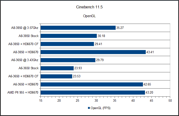
The A8-3850 manages to creep by the Phenom II in OpenGL performance when both are using the GIGABYTE HD 6670 dedicated card. The A8-3850 and A6-3650 both took a very small blow using CrossFireX for this test. According to AMD, OpenGL should only use the GPU the primary display is connected to, which is the on-die GPU in this case. While it is only about 0.5 FPS difference, it shows the small overhead for CrossFireX is still there, even when only one card is in use.
3DMark11 Benchmark
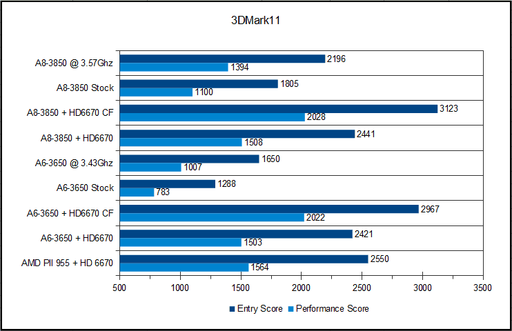
In this test, the 6MB of L3 cache won as the Phenom II 955 holds a substantial lead. When you consider the gap between the A6 and A8 is only 20E and 5P in these tests, the 109E and 56P different between the A8 and Phenom II seems huge. These are both a 300 MHz clock speed bump, and a memory bandwidth drop when moving to the Phenom II.
Media Expresso 6.5 GPU Accelerated Conversion
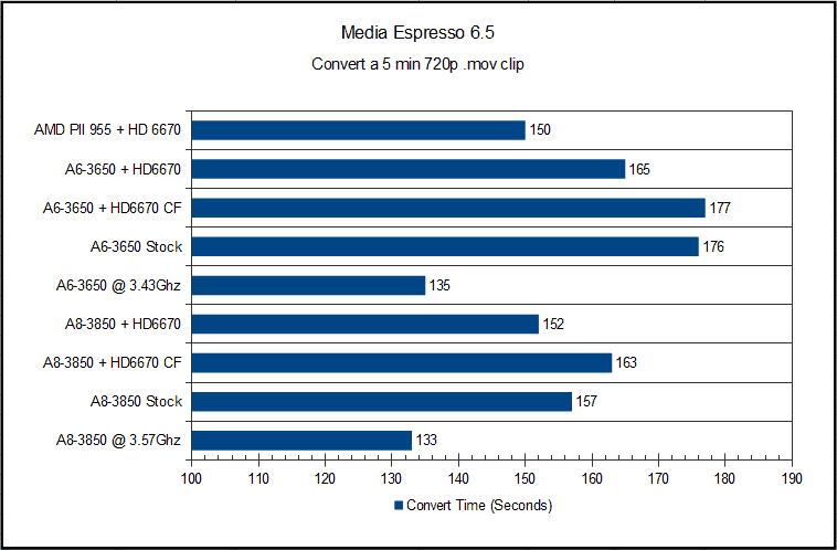
As with Handbrake, the same 5 minute 720p .mov H.264 file is converted to fit an iPhone4 with the software’s built-in preset. Once again, the CrossFireX issue we saw in the OpenGL testing comes up. This too can be a driver issue, but I am more inclined to say its a software issue in this case.
In the test where the APUs use the on-die GPU and overclocked, they are out performing the dedicated HD 6670. This should not be the case given the HD 6670 has more SIMD cores, faster clock speed, and faster memory. It cannot be an issue with CPU overhead as the faster Phenom II 955 + HD 6670 only holds a 2 second lead over to the A8-3850 + HD 6670.
Older Game Engine Test with Portal 2
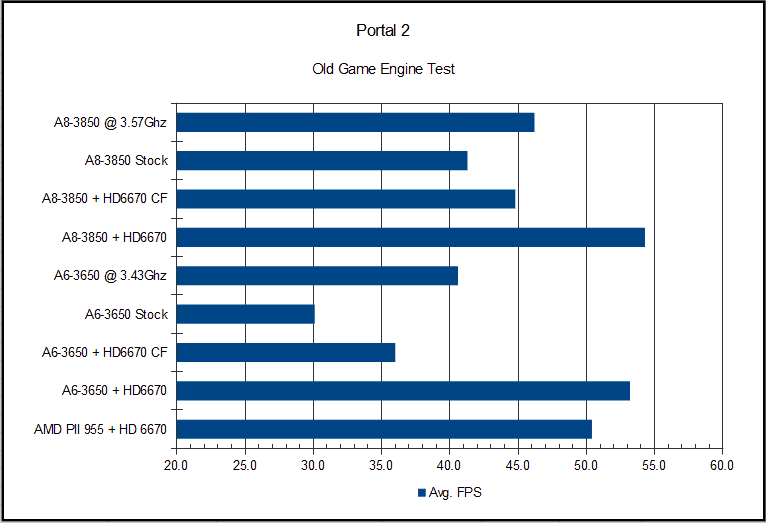
Portal 2 was tested at maxed out settings (8x MSAA, 16 x AF, Vsync ON, Very High Texture). AMD states when CrossFireX is enabled but cannot be used, the system should default to the faster of the two GPUs. This is simply not the case as the CF test are closer to the on-die GPU’s performance. To verify I checked the AMD Resource Monitor. It indicates only the GIGABYTE HD 6670 was at full speed, but the on-die GPU processor was doing most of the work. This could just be an issue with the Resource Monitor.
Resident Evil 5 Benchmark
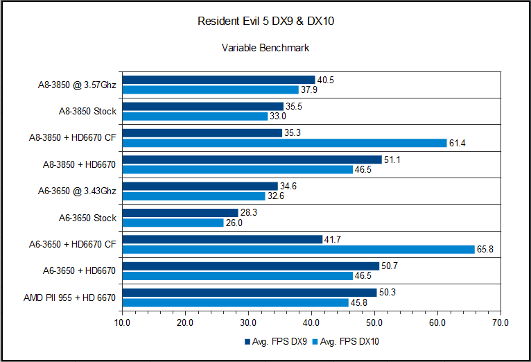
In the Resident Evil 5 DX10 tests I have full use of CrossFireX. Both the A6-3650 and A8-3850 with the GIGABYTE HD 6670 in CrossFireX broke 60 FPS average. A 25% boost in performance over just the HD 6670. In the DX9 tests, CF results were almost identical to the 6550D. It was the CF tests with the 6530D which results in performance closer to the HD 6670. It almost split the difference between the on-die 6530D and the dedicated HD 6670.
Alien Vs. Predator DirectX 11 Benchmark
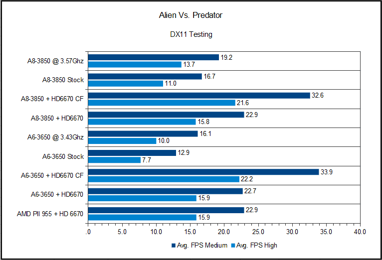
AvP was tested with the default of 16x AF, Tessellation on, Advanced Shadows on, and SSAO on. The Medium test was done with all the DX11 features turned off, 2x AF, shadows on medium, and textures on medium.
While these entry level AMD Radeon GPUs can play DX11 titles, they don’t play them very well. Even when I turn off all the DX11 features, I can barely get 30 FPS with CrossFireX enabled. Keep in mind AvP is heavily taxing in DX11 mode, so some DX11 games may be playable with an APU CrossFireX setup.
Power Consumption
These numbers are for total power consumed. The tests were done at the wall socket and corrected according to the tested efficiency of the Antec HCP 850W. The efficiency measurements are an aggregate collection of data from several websites to review the Antec HCP 850W.
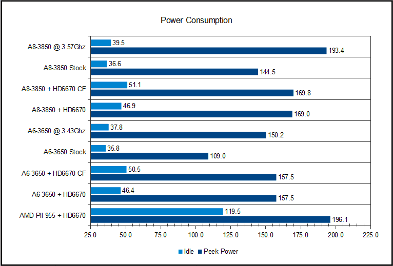
While the Phenom II does power throttle, it is nothing when compared to an APU. At idle the Phenom II 955 has a higher power draw than the A6-3650 at max load. In their idle state, the APUs quickly drop to 800 Mhz via a multiplier change and 0.9V instead of 1.4V at load. The APU makes up the 2 most power hungry components in a computer, so you get a drastic drop in overall power consumption at idle. It is also clear the extra 80 SIMPs and 4 texture units in the 6550D does come at the cost of slightly higher power draw.
Final Thoughts
The CPU side of this chip is a die shrunken version of the AMD Athlon II processors with twice the cache and an improved memory controller. While they help to get performance closer to a Phenom II, there is a gap. There is no perceivable difference in performance when you are just browsing the web, listing to music, writing documents, or playing web games.
Graphics performance is another story. The 6550D and 6530D are hands down the most powerful IGPs on the market. Futurelooks i7 2600k and i5 2500k review shows in Resident Evil 5 DX10 at 720p, the Intel 3000 IGP can only give a meager 17.4 FPS. The A6-3650 on-die 6530D can play Resident Evil 5 DX10 at 1080p at 30.1 FPS.
As for price, you can build a cheaper system with similar performance using an AM3 board at around $45, a $90 AMD Propus, and an HD 6570 for $70, totaling to $205. An A8-3850 and the GIGABYTE A75M-UD2H in my test total to $240. The extra $35 gets you four native USB 3.0 ports, five SATA III (6 Gb/s), and a better memory controller.
The only down side to an APU based PC is the current lack of upgrade paths. AMD has plans for several forthcoming APUs including a Bulldozer APU named Trinity, but it is not clear if new APUs will use the same FM1 socket.
The A8-3850 (MSRP of $139.99) and the A6-3650 (MSRP of $119.99) are well worth every dime, especially since you get the equivalent of a $70 dedicated GPU on-board. If you are on a strict budget, want to build a powerful small form factor PC, or plan to play games on a PC you bought from a retailer, the AMD Llano APUs are what you want to own. An APU PC also can be a very compelling “daily driver” system that complements a powerful Sandy Bridge or even an AMD Phenom II X6 system you use for games and/or heavy lifting.
If you already have your AMD APU based system and are still looking for a bit more performance, start with your RAM as it seems to improves everything, not just graphics. We’ll be looking at this aspect of performance in another article.
I don’t think you can be anything but surprised with this platform. Especially once you get either APU plugged in and working as a daily driven system. I know a few of us at Futurelooks have been pleasantly surprised, especially with the lack of noise and heat. AMD’s latest APU platforms certainly represent a new way of looking at value and come highly recommended from Futurelooks.
Pros
- Unparalleled Integrated Graphics Performance
- Much Improved Memory Controller
- Priced Well
- Low Power Use
- CrossFireX Support in DX10 and DX11
- Complemented Well by Hudson FCH
- Eyefinity up to 3 Monitors
Cons
- No CrossFireX Support in DX9
- Crossfire Drivers Need Work
- Small Performance Improvement over Athlon II CPUs
- Unique Socket Limits Upgrade Paths
Overall Score: 8.5 / 10


Help Us Improve Our Reviews By Leaving a Comment Below!
AMD’s Llano A8-3850 and A6-3650 APUs – The New King of Entry Level PCs – Photo Gallery